Toward practical applications from innovative core technologies created by Tohoku University, we have managed the international industry-academic consortium (CIES Consortium) consisting of seven industry–academic collaborations, and three major national projects (JST-ACCEL, ImPACT and NEDO projects) through our cooperation with a diverse range of Japanese and foreign companies from fields such as materials, equipment, devices, circuits and systems. CIES constructed the second such base for collaborative research between industry and academia in the world to be organized by a university for this academic area (other being in the U.S., and world first for the spintronics area) with first 300mm wafer process line and facilities for device characterization & physical analysis in Japanese university. CIES produced remarkable results, especially, recognized worldwide as research center for practical application of spintronics-based LSI with dozens of Japanese and foreign companies participating.
Recently, we have achieved a high performance interface type perpendicular-anisotropy magnetic tunnel junction (p-MTJ) stack, which is a key building block of spin transfer toque magnetoresistive random access memory (STT-MRAM), one of the most promising non-volatile memories. p-MTJ with CoFeB free layer and Co/Pt multilayer based synthetic ferrimagnetic (SyF) pinned layer has been developed to allow annealing at a temperature up to 420°C that compatible with complementary metal-oxide-semiconductor (CMOS) back end of line (BEOL) process by controlling boron diffusion for the first time. We demonstrated the 10 nmφ p-MTJ with double CoFeB/MgO interface tolerable against 400°C annealing which is a requisite building block for realization of high density STT-MRAM in reduced dimensions. The progress enables us to step toward the practical use of spintronics-based LSI. Figure summarizes previous studies that were classified in a thermal tolerance and MTJ size. We demonstrated 10 nmφ MTJ after 300℃ annealing reported at a world authoritative International Electron Device Meeting (IEDM) in 2013. Recently, we reported the smallest 10nm p-MTJ with highest thermal tolerance over 400℃ at IEDM2014. The p-MTJ with highest thermal tolerance was is required to get a fabrication process margin and smaller MTJ is needed to achieve high density MRAM at last.
In addition to the progress, Keysight Technologies, Inc. announced development of new STT-MRAM test solution based on collaboration with CIES (http://www.tohoku.ac.jp/en/news/research/news20150317_1.html). From above-mentioned, CIES has accelerated the research and development for practical application of spintronics based on the successful results in view of the production phase.
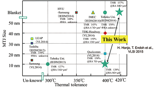
Figure Thermal tolerance vs. p-MTJ size. Most Small 10nm p-MTJ with highest thermal tolerance over 400℃ is achieved.
Reference(s):
1)H. Honjo, H. Sato, S. Ikeda, S. Sato, T. Watanabe, S. Miura, T. Nasuno, Y. Noguchi, M. Yasuhira, T. Tanigawa, H. Koike, M. Muraguchi, M. Niwa, K. Ito, H. Ohno and T. Endoh, "10nm perpendicular-anisotropy CoFeB-MgO magnetic tunnel junction with over 400℃ high thermal tolerance by boron diffusion control", 2015 Symposium on VLSI Technology Digest of Technical Papers, T160. 2)Tetsuo Endoh, "Nonvolatile Logic and Memory Devices Based on spintronics", 2015 IEEE International Symposium on Circuits and Systems (Invited)